IDTQS3257
IDTQS3257 is HIGH-SPEED CMOS QUICKSWITCH QUAD 2:1 MUX/DEMUX manufactured by Integrated Device.
FEATURES
:
- -
- -
- -
- Enhanced N channel FET with no inherent diode to Vcc 5Ω bidirectional switches connect inputs to outputs Pin patible with the 74F257, 74FCT257, and 74FCT257T Zero propagation delay, zero ground bounce Undershoot clamp diodes on all switch and control inputs TTL-patible control inputs Available in SOIC, QSOP, and S1 packages
DESCRIPTION
:
The QS3257 is a high-speed CMOS LVTTL-patible Quad 2:1 multiplexer/demultiplexer. The QS3257 is a function and pinout patible Quick Switch version of the 74F257, 74FCT257, and the 74ALS/AS/LS257 Quad 2:1 multiplexers. The low ON resistance of the QS3257 allows inputs to be connected to outputs without adding propagation delay and without generating additional ground bounce noise. Mux/Demux devices provide an order of magnitude faster speed than equivalent logic devices. The QS3257 is characterized for operation at -40°C to +85°C.
APPLICATIONS:
- -
- -
- Logic replacement Video, audio, graphics switching, muxing Hot-swapping, hot-docking Voltage translation (5V to 3.3V) Bus funneling
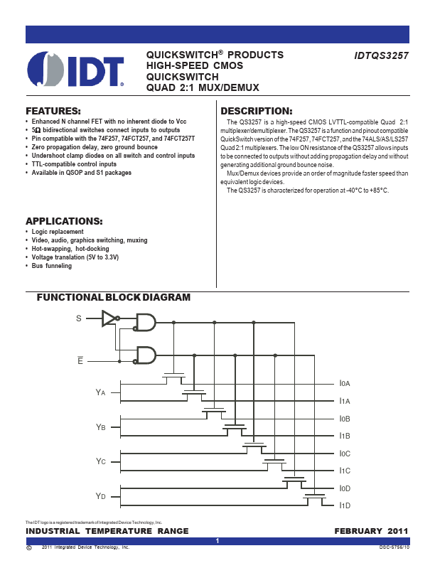
FUNCTIONAL BLOCK DIAGRAM
E I0A YA I1A I0B YB I1B I0C YC I1C I0D YD I1D
The IDT logo is a registered trademark of Integrated Device Technology, Inc.
INDUSTRIAL TEMPERATURE RANGE
1 c 2001 Integrated Device Technology, Inc.
FEBRUARY 2001
DSC-5756/6
IDTQS3257 HIGH-SPEED CMOS QUICKSWITCH QUAD 2:1 MUX/DEMUX
INDUSTRIAL TEMPERATURE RANGE
PIN CONFIGURATION
ABSOLUTE MAXIMUM RATINGS(1)
Symbol VTERM(2) VTERM(3) Description
Supply Voltage to Ground DC Switch Voltage Vs DC Input Voltage VIN AC Input Voltage (pulse width ≤ 20ns) DC Output Current Maximum Power Dissipation (TA = 85°C) Storage Temperature Max
- 0.5 to +7
- 0.5 to +7
- 0.5 to +7
- 3 120 0.5
- 65 to +150 Unit V V V V m A W °C
S I0A I1A YA I0B I1B YB GND
1 2 3 4 5 6 7 8
SOIC/ QSOP/ S1 TOP VIEW
16 15 14 13 12 11 10 9
VCC E I0D I1D YD I0C I1C YC
VTERM(3) VAC IOUT PMAX TSTG
NOTE: 1. Stresses greater than those listed under ABSOLUTE MAXIMUM RATINGS may cause...